



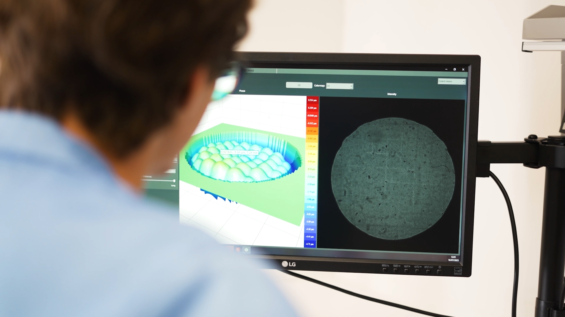
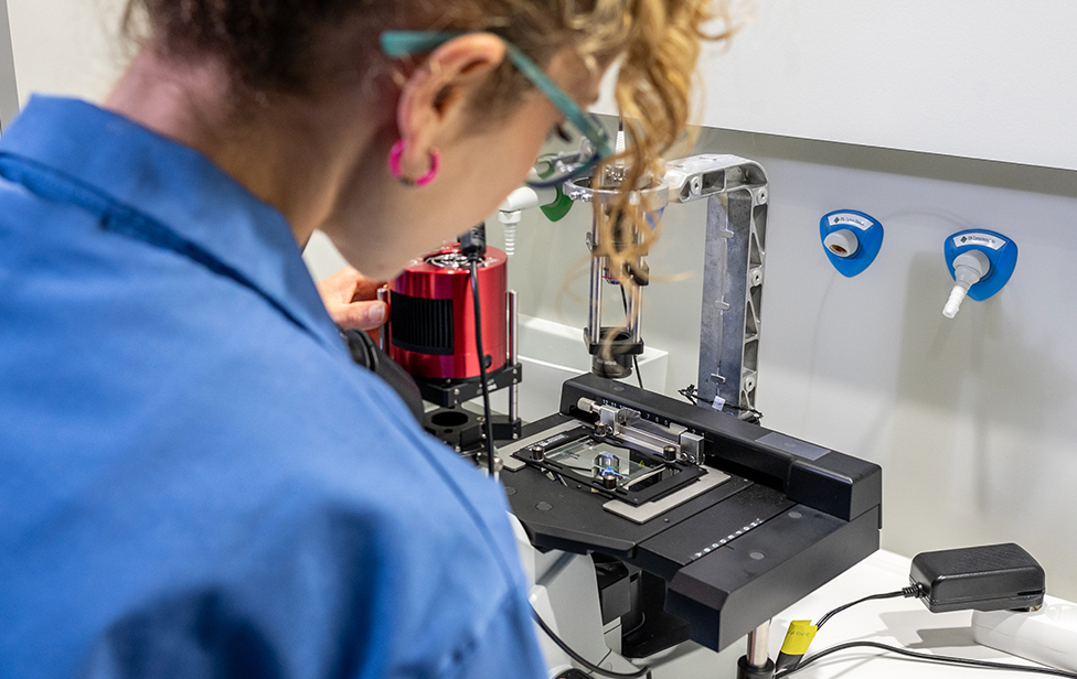
SEBI® RT1000 is a high-resolution wavefront sensor with real-time processing capabilities, specifically designed for the most demanding optical metrology and semiconductor inspection tasks, offering high-precision measurements and high-density sampling capabilities.
It inherits the core adaptive optical wavefront phase technology of Wooptix, enabling rapid capture and analysis of wavefront aberrations in optical systems. It is widely used in semiconductor wafer inspection, aberration analysis, and quality control of high-end optical systems such as endoscopes and precision lenses.
-
Core advantage
· Ultra-high-definition high-resolution sampling
· Faster real-time processing and acquisition
· Ultimate measurement accuracy and repeatability
· Wide dynamic range and wavelength adaptation
· High compatibility and ease of use
· Multi-scenario adaptability


-
Wavefront and optical performance parameters
1. Wavefront phase distribution, wavefront distortion (low-order/high-order aberrations, including spherical aberration, coma, astigmatism, field curvature, distortion, etc., decomposed using Zernike modes)
2. Optical path difference and optical path difference distribution diagram, with a minimum detectable optical path difference of<1nm
3. Optical element transmittance/reflectance, light intensity distribution and uniformity
4. Lens surface shape error, edge quality, uniformity, and roughness (capable of detecting surface roughness ranging from 2.5nm to 20nm)
5. Auxiliary analysis of modulation transfer function (MTF) of optical system, imaging resolution to edge consistency
-
Material and sample morphology parameters
1. Sample surface nano-morphology, three-dimensional profile, and topological map
2. Surface roughness, local stress distribution, and deformation
3. Thickness, total thickness variation, and global flatness of transparent/reflective samples
4. Microstructure size and precision (such as microlens arrays, line width of lithographic patterns, edge roughness)
-
Dynamic processes and biological sample parameters
1. Real-time phase changes of dynamic samples (such as laser ablation, nanoimprint, and coating wetting processes)
2. Label-free quantitative phase imaging of biological cells/tissues, cell dry mass/volume/dynamic motion trajectory
3. Fluid motion, particle size and distribution measurement of micro-particles in microfluidic chips
-
Exclusive parameters for optical element characterization
1. Ring defects, deformation, uniformity, and surface roughness of intraocular lenses (IOLs);
2. The inner surface roughness and surface morphology of polished metal components, such as titanium alloy prostheses;